
The ₹1.27 lakh crore India Semiconductor Mission 2.0 aims to transform India into a global semiconductor powerhouse. By fostering chip design, fab establishment, and ATMP infrastructure, it strengthens technological sovereignty, drives economic growth, and mitigates global supply chain dependencies.
Why In News?
The Union Cabinet, chaired by the Prime Minister, approved India Semiconductor Mission (ISM) 2.0 to transform India into a global semiconductor hub.
What is India Semiconductor Mission (ISM) 2.0?
ISM 2.0 is designed to build a semiconductor ecosystem, advancing beyond basic fabrication to include domestic chip design, precision manufacturing, advanced packaging, and intellectual property (IP) creation.
The Indian government shifted its strategy from basic ecosystem creation under ISM 1.0—which sanctioned 12 manufacturing units with over ₹1.64 lakh crore in investments—to deep ecosystem integration under ISM 2.0 to mitigate global supply chain vulnerabilities and ensure technological sovereignty.
Why is ISM 2.0 Important for India?
Import Substitution: The mission localizes production to reduce India's reliance on a handful of nations for over 70% of its defense and critical infrastructure semiconductors, mitigating exposure to global export controls and technology denial regimes.
Technological Sovereignty: ISM 2.0 ensures that India owns the fundamental technology layers—from logic algorithms to silicon fabrication—preventing adversaries from exploiting hardware backdoors or supply chain disruptions.
Electronics Manufacturing Growth: The initiative drives the domestic semiconductor market toward a projected USD 100–110 billion valuation by 2030 by accelerating domestic capital investment and positioning India as a primary supplier in the global technology value chain.
National Security Capabilities: The program produces ruggedized, secure gallium nitride (GaN) and gallium arsenide (GaAs) components essential for radars, electronic warfare, missile seekers, and secure military communications.
Global Supply Chain Integration: The mission leverages the geopolitical "China Plus One" strategy to anchor India as a trusted, long-term alternative manufacturing hub for global chip supply.
Digital Economy Expansion: The framework fosters the creation of proprietary AI-native processors, driving innovation in on-device AI computing, electric mobility, telecommunications, and 6G networks.
What are the Key Features of ISM 2.0?
Financial Outlay: The Union Cabinet allocates ₹1,27,500 crore to fund the six foundational pillars of the semiconductor ecosystem.
Capital Subsidies: The policy provides capital subsidies, offering 40% support for silicon fabs and 35% support for display and compound semiconductor fabs to accelerate the establishment of new fabrication units.
Upstream Supply Chain Incentives: The government guarantees a 30% financial incentive for companies manufacturing semiconductor equipment, specialty chemicals, and gases to localize the upstream supply chain.
Design-Linked Innovation: Supports startups with financial grants, equity co-investments, and access to expensive industry-standard Electronic Design Automation (EDA) tools to develop strategic IP.
Advanced Packaging Support: Promotes the Outsourced Semiconductor Assembly and Test (OSAT) and Assembly, Testing, Marking, and Packaging (ATMP) sectors, offering 35% incentives for advanced packaging facilities to attract cutting-edge technologies.
Talent Development Framework: Partners with universities to train students in complex chip design, providing up to 75% financial assistance to academic setups to deepen talent generation in cleanroom operations and fab construction.
What are the Major Concerns Associated with Semiconductor Manufacturing?
High Capital Intensity: Semiconductor fabrication is a capital-intensive heavy industry, requiring billions of dollars upfront and long-term financial commitments before yielding viable returns.
Technology Transfer Barriers: India faces technology denial regimes and ITAR ((International Traffic in Arms Regulations)-related import restrictions, limiting access to advanced Western semiconductor technologies and defense-grade fabrication hardware.
Supply Chain Dependencies: Domestic fabs remain dependent on foreign imports for raw materials, including photoresists, rare earth elements, and chemical mechanical planarization (CMP) slurries controlled predominantly by China.
Skilled Talent Deficit: India experiences faculty shortages in advanced semiconductor disciplines, as academia heavily favors software over hardware and lacks scalable, high Technology Readiness Level (TRL) hardware patents.
Ecological and Infrastructure Toll: Fabs demand uninterrupted power grids and massive quantities of Ultra-Pure Water (UPW), which exacerbates water stress in industrial states like Gujarat and Maharashtra.
Rapid Technological Obsolescence: Hyper-rapid global innovation cycles shorten the commercial lifespan of newly established facilities, requiring complex scaling from legacy mature nodes (28nm) to advanced sub-5nm nodes.
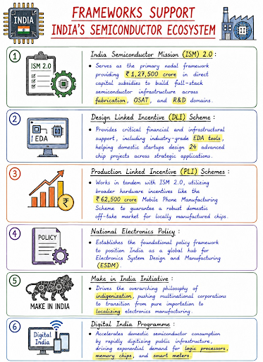
What Measures Can Help India Become a Global Semiconductor Hub?
R&D Transition: Accelerates R&D transition from mature legacy nodes (28nm-110nm) to advanced architectures, pioneering AI-native designs, silicon photonics, and neuromorphic computing.
Talent Pipeline Integration: Institutionalizing defense-funded PhD programs, expanding shared fabrication facilities for student testing, and prioritizing high-level hardware design training over generic software skills.
International Strategic Partnerships: Leverages Quad-based initiatives to aggregate technologies from friendly nations, securing Japanese material science expertise, Taiwanese advanced packaging, and American fabless ecosystem frameworks.
Precision Manufacturing Clusters: Establish dedicated manufacturing clusters incorporating structured "urban mining" and e-waste recycling, aiming to fulfill 20–30% of critical material needs independently by recovering rare-earth elements from domestic electronic waste.
Long-Term Policy Stability: Prioritizing direct upfront capital subsidies over delayed operational concessions, assuring domestic and global investors of permanent state backing.
Environmental Safeguards: Pairs component manufacturing incentives with strict Zero Liquid Discharge (ZLD) safeguards to manage hazardous waste streams, potent greenhouse gases, and "forever chemicals" utilized in fabrication.
Conclusion
The India Semiconductor Mission (ISM) 2.0 shifts India from a dependent consumer to an indispensable global technology node by synergizing robust capital subsidies, strategic R&D, and trusted international partnerships to achieve technological sovereignty.
Source: IBEF
|
PRACTICE QUESTION Q. "Semiconductors have emerged as the foundation of economic competitiveness, technological leadership and national security in the twenty-first century." Discuss (250 Words, 15 Marks) |





© 2026 iasgyan. All right reserved