India’s ₹1,943 crore Odisha unit advances technological sovereignty. Using 3D glass packaging to bypass silicon limits, it pivots India toward high-value manufacturing. Success requires overcoming supply chain gaps and talent deficits.
Why In News?
The Union Cabinet approved India’s first 3D glass semiconductor packaging unit in Bhubaneswar, Odisha.
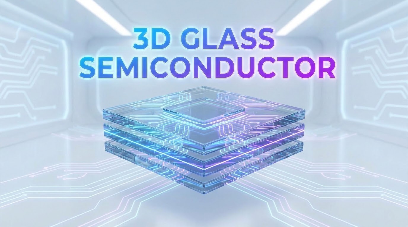
About 3D Glass Semiconductor Project
The facility represents a transition from traditional semiconductor materials to high-performance glass-based solutions.
Investment: Approximately ₹1,943 crore.
Technology Partner: The unit is being established by Heterogeneous Integration Packaging Solutions (HIPS), a subsidiary of the US-based 3D Glass Solutions (3DGS).
Capacity: The plant is designed to produce 70,000 glass panels and 50 million assembled units annually.
Strategic Location: Situated in Info Valley, Bhubaneswar, leveraging Odisha’s emerging status as a tech-manufacturing hub.
It involves stacking different types of chips (logic, memory, sensors) vertically on a single base. Glass serves as the "interconnect" layer that allows these chips to talk to each other.
Advantages of Glass Over Silicon/Organic Materials
Thermal Stability: Glass maintains its shape under extreme heat, preventing the "warping" common in plastic substrates during high-intensity AI processing.
Signal Integrity: Glass allows for faster data transmission with lower power loss, which is essential for 5G/6G and Satellite Communication.
Density: It enables a higher density of "vias" (vertical holes for electrical connections), allowing more transistors to be packed into a smaller space.
Advancing the Value Chain
India is expanding from Chip Design into high-margin "Advanced Packaging." This transition addresses a historical lack of domestic Fabrication and Packaging capability.
Strategic Autonomy
The facility produces Radio Frequency (RF) filters and modules vital for Defense and Aerospace, strengthening national security by reducing import reliance.
Part of the India Semiconductor Mission (ISM)
The ISM is a specialized business division within the Digital India Corporation with a total outlay of ₹76,000 crore.
Source: INDIAN EXPRESS
|
PRACTICE QUESTION Q. What is the primary technical advantage of "3D Glass Semiconductor Packaging" over traditional silicon-based packaging? A. Lower transparency for optical sensors B. Higher thermal stability and superior vertical component stacking for AI processing C. Higher flexibility for wearable consumer electronics D. Use of organic materials to reduce electronic waste Answer: B Explanation: Glass substrates allow for higher-density vertical stacking, superior heat management for powerful AI processors, and reduced electrical signal loss, making them superior to traditional 2D silicon layouts in high-performance computing scenarios. |
3D glass semiconductors are advanced microchips where diverse components (like logic, memory, and sensors) are stacked vertically on glass substrates instead of being spread flat on a traditional 2D silicon plane. This architecture allows for much higher computing speeds, better cooling, and enhanced performance within a microscopic footprint.
Glass is highly stable under extreme heat, reduces electrical signal loss, and allows chip interconnects to be placed much closer together. This makes it an ideal material for handling the massive amounts of data and extreme speeds required by modern AI data centers and 5G networks without overheating.
The India Semiconductor Mission (ISM) is a government initiative aimed at building a robust, self-reliant domestic semiconductor and display ecosystem. It provides capital subsidies and policy support to transition India from a heavy importer of electronic components to a high-value, advanced technological manufacturer.


© 2026 iasgyan. All right reserved