Nanophotonics enables trapping infrared light in layers 1,000 times thinner than hair using Molybdenum Diselenide. This breakthrough overcomes the diffraction limit, facilitating ultra-fast, heat-free optical computing and thin night-vision sensors through large-scale Molecular Beam Epitaxy manufacturing.
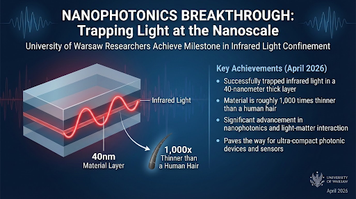
Researchers from the University of Warsaw achieved a milestone in nanophotonics by successfully trapping infrared light in a layer of material only 40 nanometers thick—roughly 1,000 times thinner than a human hair.
Nanophotonics is the study of light’s behavior on the nanometer scale and its interaction with nanostructures.
Key Components of the Discovery
The Material: Molybdenum Diselenide (MoSe2)
Optical Computing: Transitioning from electrons to photons means data can move at the speed of light. These chips generate almost zero heat, solving the thermal throttling issues faced by current silicon processors.
Night Vision & Sensing: Breakthrough demonstrated Third Harmonic Generation (THG), where three infrared photons were combined to create a single blue (visible) photon. This could lead to paper-thin night vision films for glasses or car windshields.
Telecommunications (6G): Future 6G networks will require terahertz frequencies. Nanophotonic filters and modulators will be essential for handling these massive bandwidths in compact devices.
Source: REPUBLICWORLD
|
PRACTICE QUESTION Q1. With reference to 'Molybdenum Diselenide (MoSe₂)', often seen in news, consider the following statements:
Which of the statements given above is/are correct? A) 1 only B) 1 and 2 only C) 2 and 3 only D) 1, 2 and 3 Answer: B Explanation: Statement 1 is correct: Molybdenum Diselenide belongs to the class of Transition Metal Dichalcogenides (TMDs), which are layered materials consisting of a transition metal (like Molybdenum) sandwiched between two chalcogen atoms (like Selenium). Statement 2 is correct: Molybdenum Diselenide has an exceptionally high refractive index (slowing light by about 4.5 times compared to 1.5 in glass), which allows it to trap and confine light efficiently at the nanoscale, even in layers 1,000 times thinner than a human hair. Statement 3 is incorrect: Contrary to being impossible to produce at scale, recent advancements have demonstrated scalable production methods for Molybdenum Diselenide thin films, such as molecular beam epitaxy (MBE) and chemical vapor deposition (CVD), making it viable for industrial and real-world applications in photonics and electronics. |
Nanophotonics is the study and manipulation of light on a nanometer scale. It involves using ultra-thin materials to control light waves, enabling the creation of microscopic optical devices like Photonic Integrated Circuits (PICs).
The diffraction limit is a fundamental physical constraint. Conventionally, to confine a light wave effectively, a device's size must be comparable to the light's wavelength. Overcoming this limit allows scientists to trap light in material structures much thinner than the light's actual wavelength.
MoSe2 is a Transition Metal Dichalcogenide (TMD) with an exceptionally high refractive index of roughly 4.5. This high density drastically slows down light passing through it, allowing the material to trap and hold infrared light within a microscopic space just 40nm thick.


© 2026 iasgyan. All right reserved