Disclaimer: Copyright infringement not intended.
Context
- The Centre approved changes to the Modified Special Incentive Package Scheme (M-SIPS) scheme for the development of a semiconductor and display manufacturing ecosystem in the country.
M-Sips
About
- Modified Special Incentive Package Scheme (M-SIPS) is an incentive scheme launched by the Government of India in 2012.
Aim and Objective
- Aim of the Scheme is to attract investments and boost production in the electronics goods industry.
- The purpose of initiating Modified Special Incentive Package Scheme (M-SIPS) was not only to encourage investments but also to generate employment opportunities.
In a nutshell,
The objectives of this scheme are as follows -
- Attract investment in the Electronics System Design & Manufacturing.
- Boosting the production of electronics goods by developing electronic manufacturing units.
- Making India self-sufficient to fulfil India’s domestic demand for electronic items.
- Employment generation.
Features of Modified Special Incentive Package Scheme
- This scheme provides a capital subsidy to the investors of SEZ and non-SEZ.
- Both new and expanding electronic manufacturing units receive incentives.
- Reimbursement on excise duties and central tax is available for high capital investment units.
Mechanism
- The incentive under the M-SPIC scheme is in the form of subsidy and is available for a startup project, the expansion of the project (in terms of capital invested) or the diversification of project (variation in the range of products).
- The Government offers a subsidy of 20% on investments in special economic zones (SEZs) and 25 per cent on capital investments in non-SEZs.
- The incentives are provided reimbursement basis (i.e.) subsidy claimed after investments have been made and are available for ten years from the date of approval. Reimbursement of central taxes and duties is obtainable for projects with high capital investment. This scheme also provides incentives to relocate units from abroad to India.
Benefits of Modified Special Incentive Package Scheme
- Investors will receive a 20% capital subsidy for investing in Special Economic Zones (SEZs).
- They will receive a 25% of the same for units out of Special Economic Zones.
- Incentives will be available for 44 categories of products across the value chain. Those include raw materials from the assembly, testing, and packaging. In addition, the product verticals also comprise raw material for chips, accessories and components.
- These incentives will be available for the next 10 years of the approval of the application.
- This scheme also provides reimbursement of excise for capital assets for the non-SEZ units.
- Hi-tech and giant asset investment units will also receive central duties and taxes reimbursement.
Who Are Eligible for Modified Special Incentive Package Scheme
- Investors must invest a minimum of ₹ 1 crore for accessories manufacturing to apply for this scheme. Additionally, a minimum ₹ 5000 crores threshold should be for semiconductor fabrication units.
- The units must be in the industrial area notified by the Central or State Government.

Revision of MSIPS in July, 2015
- Under the “Digital India” Programme and the “Make in India” Programme, the scheme attained renewed vigor.
- Several new domestic and global majors entered into the field of electronics manufacturing in the country and submitted their investment proposals under the scheme.
- Simplification of procedures: The Government made it easier to receive benefits under the scheme namely, allowing M-SIPS incentives from the date of submission of application, allowing disbursement of incentives on a quarterly basis as against annual basis under the earlier scheme, dispensation of separate technical evaluation and allowing MSIPS in any part of the country as against only in notified areas etc.
Further amendments in January, 2017
- To expedite the investments in the sector, the scheme was further amended. Vide these amendments, the incentives were made available for a period of 5 years from the date of approval of the project (instead of 10 years).
Program For the Development Of Sustainable Semiconductor And Display Ecosystem
- In furtherance of the vision of Aatmanirbhar Bharat and positioning India as the global hub for Electronics System Design and Manufacturing, the Cabinet had approved the comprehensive program for the development of sustainable semiconductor and display ecosystem in the country.
- The programme aims to provide attractive incentive support to companies / consortia that are engaged in Silicon Semiconductor Fabs, Display Fabs, Compound Semiconductors / Silicon Photonics / Sensors (including MEMS) Fabs, Semiconductor Packaging (ATMP / OSAT) and Semiconductor Design.
Incentives approved for the development of semiconductors and display manufacturing ecosystem in India
- Semiconductor Fabs and Display Fabs: The Schemes for Setting up of Semiconductor Fabs and Display Fabs in India shall extend fiscal support of up to 50% of project cost on pari-passu basis to applicants who are found eligible and have the technology as well as capacity to execute such highly capital and resource intensive projects. Government of India will work closely with the State Governments to establish High-Tech Clusters with requisite infrastructure in terms of land, semiconductor grade water, high quality power, logistics and research ecosystem to approve applications for setting up at least two greenfield Semiconductor Fabs and two Display Fabs in the country.
- Semi-conductor Laboratory (SCL): Union Cabinet has also approved that Ministry of Electronics and Information Technology will take requisite steps for modernization and commercialization of Semi-conductor Laboratory (SCL), Mohali. MeitY will explore the possibility for the Joint Venture of SCL with a commercial fab partner to modernize the brownfield fab facility.
- Compound Semiconductors / Silicon Photonics / Sensors (including MEMS) Fabs and Semiconductor ATMP / OSAT Units: The Scheme for Setting up of Compound Semiconductors / Silicon Photonics / Sensors (including MEMS) Fabs and Semiconductor ATMP / OSAT facilities in India shall extend fiscal support of 30% of capital expenditure to approved units. At least 15 such units of Compound Semiconductors and Semiconductor Packaging are expected to be established with Government support under this scheme.
- Semiconductor Design Companies: The Design Linked Incentive (DLI) Scheme shall extend product design linked incentive of up to 50% of eligible expenditure and product deployment linked incentive of 6% - 4% on net sales for five years. Support will be provided to 100 domestic companies of semiconductor design for Integrated Circuits (ICs), Chipsets, System on Chips (SoCs), Systems & IP Cores and semiconductor linked design and facilitating the growth of not less than 20 such companies which can achieve turnover of more than Rs.1500 crore in the coming five years.
- India Semiconductor Mission: In order to drive the long-term strategies for developing a sustainable semiconductors and display ecosystem, a specialized and independent “India Semiconductor Mission (ISM)” will be set up. The India Semiconductor Mission will be led by global experts in semiconductor and display industry. It will act as the nodal agency for efficient and smooth implementation of the schemes for setting up of Semiconductor and Display Fabs.
Recent Modifications in the Programme
The Government has approved the following modifications in the Programme for development of semiconductors and display manufacturing ecosystem in India:
- Fiscal support of 50% of Project Cost on pari-passu basis for all technology nodes under Scheme for Setting up of Semiconductor Fabs in India.
- Fiscal support of 50% of Project Cost on pari-passu basis under Scheme for Setting up of Display Fabs.
- Fiscal support of 50% of Capital Expenditure on pari-passu basis under Scheme for Setting up of Compound Semiconductors / Silicon Photonics / Sensors Fab and Semiconductor ATMP /OSAT facilities in India. Additionally, target technologies under the Scheme will include Discrete Semiconductor Fabs.
- Under modified programme, a uniform fiscal support of 50% of Project Cost shall be provided across all technology nodes for setting up of Semiconductor Fabs. Given the niche technology and nature of compound semiconductors and advanced packaging, the modified programme shall also provide fiscal support of 50% of Capital Expenditure in pari-passu mode for setting up of compound semiconductors / silicon photonics / sensors / Discrete semiconductors fabs and ATMP/OSAT.
Significance
- The programme has attracted many global semiconductor players for setting up fabs in India. The modified programme, will expedite investments in semiconductor and display manufacturing in India. On the basis of discussion with potential investors, it is expected that work on setting up of the first semiconductor facility will commence soon.
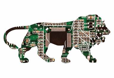
Semiconductor
- Semiconductors, or chips, have properties that are somewhere between conductors and insulators.
- Usually made of silicon,they are used to power a wide range of devices - cars, laptops, smart-phones, household appliances and gaming consoles.
- These tiny objects perform a host of functions such as powering displays and transferring data.
- So, a supply crunch has a consequent impact on sales of cars, fridges, laptops, TVs and other electronic devices.
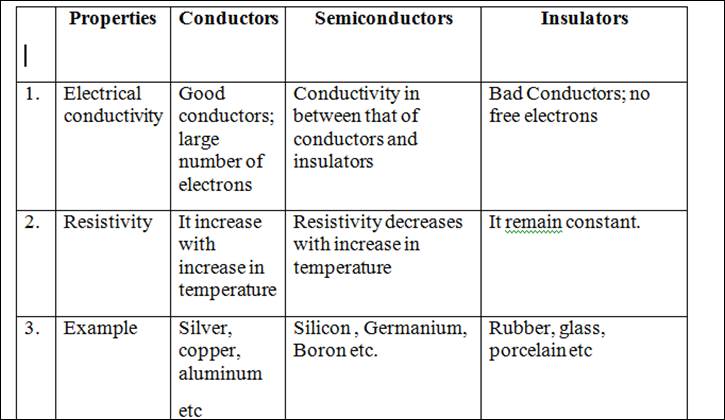
- Semiconductors are the thumbnail-sized building blocks of almost every modern electronic device from smartphones to connected devices in the Internet of Things (IoT).
- The basic component of a semiconductor chip is a sliver of silicon, which is etched with billions of microscopic transistors and projected to specific minerals and gases, forming patterns to control the flow of current while following different computational instructions.
- The most-advanced semiconductor, developed in 2020 is known as the 5nm, having 16 billion transistors. Semiconductors having higher nanometre value are applied in automobiles, consumer electronics and so on, while those with lower values are used in devices such as smartphones and laptops.
Complex Chip making Process
- The chip-making process is complex and highly exact, having multiple other steps in the supply chain such as chip-designing done by companies to develop new circuitry for use in appliances, designing software for chips and patenting them through core Intellectual Property (IP) rights. It also involves making chip-fabrication machines; setting up fabs or factories; and ATMP (assembly, testing, marking and packaging).
- Manufacturing advanced logic chips requires extraordinary precision,along with huge long-term bets in a field subject to rapid change.
- Manufacturing a chip typically takes more than three months and involves giant factories, dust-free rooms, multi-million-dollar machines, molten tin and lasers.
- Plants cost billions of dollars to build and equip, and they have to run flat-out 24/7 to recoup the investment.
- A factory also gobbles up enormous amounts of water and electricityand is vulnerable to even the tiniest disruptions, whether from dust particles or distant earthquakes.
Basic Requirements for Chip Facility
- A clean environment, i.e, low air particulate matter,
- Abundant supply of clean, fresh water,
- Uninterrupted and stable power supply,
- Quick access to an international airport or seaport,
- First-world levels of road infrastructure from the said port to the fab
- Close proximity to well-trained technical talent
Global Semiconductor Industry Scenario
- The global semiconductor industry is currently valued at $500-$600 billion and caters to the global electronics industry currently valued at about $3 trillion.
- The chip-making industry is a highly-concentrated one, with the big players being Taiwan, South Korea and the U.S. among others.
- 90% of 5nm (nanometre) chips are mass-produced in Taiwan. Taiwan holds a virtual monopoly in the global chip manufacturing industry.
Global Chip Shortage
- The global chip shortage, S.-China tensions over Taiwan, and the supply chain blockages owing to the Russia-Ukraine conflict have led major economies to enter the chip-making sector with a renewed push.
- Palladium and neon are two resources that are key to the production of semiconductor chips.
- Now that Russia supplies over 40 per cent of world’s palladium and Ukraine produces 70 per cent of neon, there can be global chip shortage to worsen if the military conflict persists.
- During the 2014-15 Crimea invasion, neon prices went up several times over, serving an indication of the seriousness of the current crisis for the semiconductor industry.
|
NEON AND PALLADIUM
Neon gas is used in the photolithography process that is the most common method for fabricating integrated circuits. Specifically, the neon gas is used in the laser machines that carve the integrated circuits. For use of neon gas in the semiconductor industry, the gas has to reach 99.99% purity levels — which makes it a rarity. More than half of semiconductor-grade neon comes from Ukrainian companies Incas and Cryoin.
Palladium is used for multiple purposes in semiconductor and electronic manufacturing. It is used to coat electrodes that help control flow of electricity. It is also used in plating of microprocessors and printed circuit boards — which is an essential process of chip making. Russia accounts for nearly half the global supplies of palladium and the multiple trade sanctions on Moscow threaten to constrain the availability of the element.
|
Challenges faced by the semi-conductor Industry:
The world's top chipmakers still can't manufacture chips fast enough to satisfy the market's insatiable appetite.
The COVID-19 crisis
- The pandemic disrupted semiconductor shipments as global demand for new mobile devices, PCs, and data center upgrades surged in response to remote work, online learning, and other stay-at-home trends.
- Lockdowns across the world forced chip-making facilities to shut in countries like Japan, South Korea, China and the US.
Declining memory chip prices
- Memory chip prices soared in 2017 and 2018, but declined in 2019 and 2020 amid sluggish demand from the PC and smartphone markets.
The ongoing tech war
- The tech war between the U.S. and China, which intensified under President Donald Trump and is continuing under President Joe Biden, is another pressing issue.
- The U.S. has already levied sanctions against several big Chinese companies, including SMIC and Huawei, amid national security concerns.
- Those sanctions are exacerbating the shortage of advanced chips in China.
- They're also spurring the Chinese government to aggressively invest in its domestic chipmakers to reduce its overall dependence on overseas technologies -- which could cause a messy decoupling of the U.S. and Chinese markets.
Fluctuating forecasts
- Automakers that cut back drastically early in the pandemic underestimated how quickly car sales would rebound.
- They rushed to re-up orders late in 2020, only to get turned away because chipmakers were stretched supplying computing and smartphone giants like Apple Inc.
Stockpiling
- Chinese companies began building up inventory to ensure it could survive U.S. sanctions that were set to cut it off from its primary suppliers.
Disasters
- Several recent setbacks -- including a power outage at TSMC, a production pause at Samsung, and a fire at the Japanese auto chipmaker Renesas -- all highlight the fragility of the semiconductor supply chain.
Impact:
Disrupted supply chain
- The semiconductor shortage severely disrupts the supply chain and constrains the production of many electronic equipment types.
- Production of laptops, tablets, smartphones and other electronic devices are impacted by the shortage of semiconductors.
Increasing Prices
- Foundries are increasing wafer prices, and in turn, chip companies are increasing device prices.
Production Disruption in automobile Sector
- Domestic and global automobile manufacturers cut output and halt production due to the semiconductor shortage.
- According to data from Society of Indian Automobile Manufacturers (SIAM), automobile wholesales in India declined 11 percent year-on-year in August 2021.
- Chip shortages are expected to wipe out $210 billion of sales for carmakers in 2022, with production of 7.7 million vehicles lost.
Challenges specific to India:
Competition
- It is difficult to compete with neighbouring countries like China and Vietnam which have been favourite destinations for global chip manufacturers due to better cost-efficiency.
Massive investment
- In addition to the huge cost, running in billions of dollars, manufacturing even a single chip requires hundreds of gallons of pure water, which may also be hard to find in India in the required quantities.
- Just the setting up of one semiconductor fab requires an investment of anywhere between $3 and $7 billion.
Infrastructure
- There have been challenges in setting up of Semiconductor Wafer Fabrication (FAB) units in India.
- India is still not unto the par in terms of the basic infrastructure needed.
Power Supply
- An uninterrupted power supply is another major hurdle. With just seconds of fluctuations or spikes causing millions in losses.
- The heart of the issue is that India is still not unto the par in terms of the basic infrastructure needed to pursue endeavours in the chip manufacturing space.
Water Requirement
- Chip-making requires gallons of ultrapure water in a single day, which experts say, could be a task for the government to provide to factories, compounded also by the drought conditions which often prevail in large parts of the country.
Price pressure
- There is also constant price pressure from other global players, particularly China which is also building a homegrown chip program for the adoption of local semiconductors in 70% of its products by 2025.
Dependency on Imports
- India imports 100% of its semiconductors.
- Around 40 percent of India’s demand is met through imports from China, despite the frequent geopolitical impasse that the two nations find themselves in.
While India focuses on “lagging-edge” technology nodes in the start to supply to the automotive and appliance sector, creating global demand may be difficult as giants like Taiwan offer viable cutting-edge chip-tech worldwide. Thus, attracting global players to set up here would be beneficial as they come with their customer base.
Government Efforts:
Development of sustainable semiconductor and display ecosystem in the country Programme
- The comprehensive programme for the “development of sustainable semiconductor and display ecosystem in the country”is aimed at making India a global hub of electronic system design and manufacturing.
- The scheme would provide fiscal support of up to 50% of the project cost for setting up semiconductor and display fabrication units.
100% FDI in the ESDM
- In 2016, the government allows 100% FDI in the ESDM sector through an automatic route to attract investmentsincluding from Original Equipment Manufacturers (OEMs) and Integrated Device Manufacturers (IDMs).
Electronics development Fund
- The Department of Electronics and Information Technology (DeitY) has established an Electronics Development Fund (EDF) managed by Canara Bank to provide risk capital and to attract venture funds, angel funds and seed funds for incubating R&D and fostering the innovative environment in the sector.
Initiatives under Telecom and Electronic Policies
- Some of the initiatives outlined in the National Electronics policy and the National Telecom policy are in the process of implementation, such as Preferential Market Access (PMS), Electronics Manufacturing Clusters (EMC) and Modified Special Incentive Package Scheme (M-SIPS).
Scheme for Promotion of manufacturing of Electronic Components and Semiconductors (SPECS)
- Ministry of Electronics and Information Technology (MeITy) has drawn up the Scheme for Promotion of manufacturing of Electronic Components and Semiconductors (SPECS).
Production-linked incentive scheme (PLI) scheme
- Under the scheme, the Centre will offer financial support to companies that want to manufacture a range of semiconductor goods in India.
- The subsidy will bring down the production costs of companiesmanufacturing such goods, and thus encourage them to set up new factories and other facilities.
DLI Scheme
- India announced fiscal support for a design-linked initiative (DLI) scheme to drive global and domestic investment related to design software, IP rights etc.
Global Efforts
- Factories that produce wafers cost tens of billions of dollars to build, and expanding their capacity can take up to a year for testing and qualifying complex tools. In the US, the Biden administration’s $2 trillion infrastructure investment package includes $50 billion for the semiconductor industry.
- The South Korean government has announced a massive $451 billion investment to help companies boost production of semiconductors.
- Many tech companies have begun developing their own chips, a move that will not only alleviate the current supply concerns but will likely help the industry in the long-run.
- Western countries are focusing on the need to shift manufacturing within their countries and become self-reliant.
Way Ahead:
- According to the Electronics and IT Ministry, semiconductor demand in India would increase to $70-$80 billion by 2026 with the growing demand for digital devices and electronic products.
- As 5G mobile networks proliferate with many people working from home, the need for more powerful, energy-efficient chips is only going to grow.
- The rise of artificial intelligence is another force pushing innovation, since AI relies on massive data processing.
- Indian semiconductor industry is set for a stable upsurge with bright prospects provided India's generic obstacles like redtape-ism, fund crunch and infrastructural deficits are adequately addressed.
Steps needed to be taken:
- Land Acquisition by the government:acquire the land and develop a special economic zone (SEZ) which would encompass a complete semiconductor manufacturing ecosystem.
- Cover all ancillaries:The monetary benefits being extended for setting up a fab should be made available for all the ancillary units manufacturing specialty chemicals to clean room apparel.
- Focus on simple technology:The requirements are less stringent and the fabs less expensive. These companies typically operate at much lower gross margins as opposed to the large fabs and Original Equipment Manufacturer (OEMs).
- With the implementation of fabrication capabilities in India, the country could achieve a degree of self-sufficiency in the sector of semiconductors.
- Building a strong semiconductor industry would put an end to the country’s reliance on imports to meet its semiconductor needs and will help in the creation of jobs.
https://www.thehindu.com/sci-tech/technology/explained-a-push-for-the-semiconductor-industry/article65939231.ece