Copyright infringement not intended
Picture Courtesy: INDIAN EXPRESS
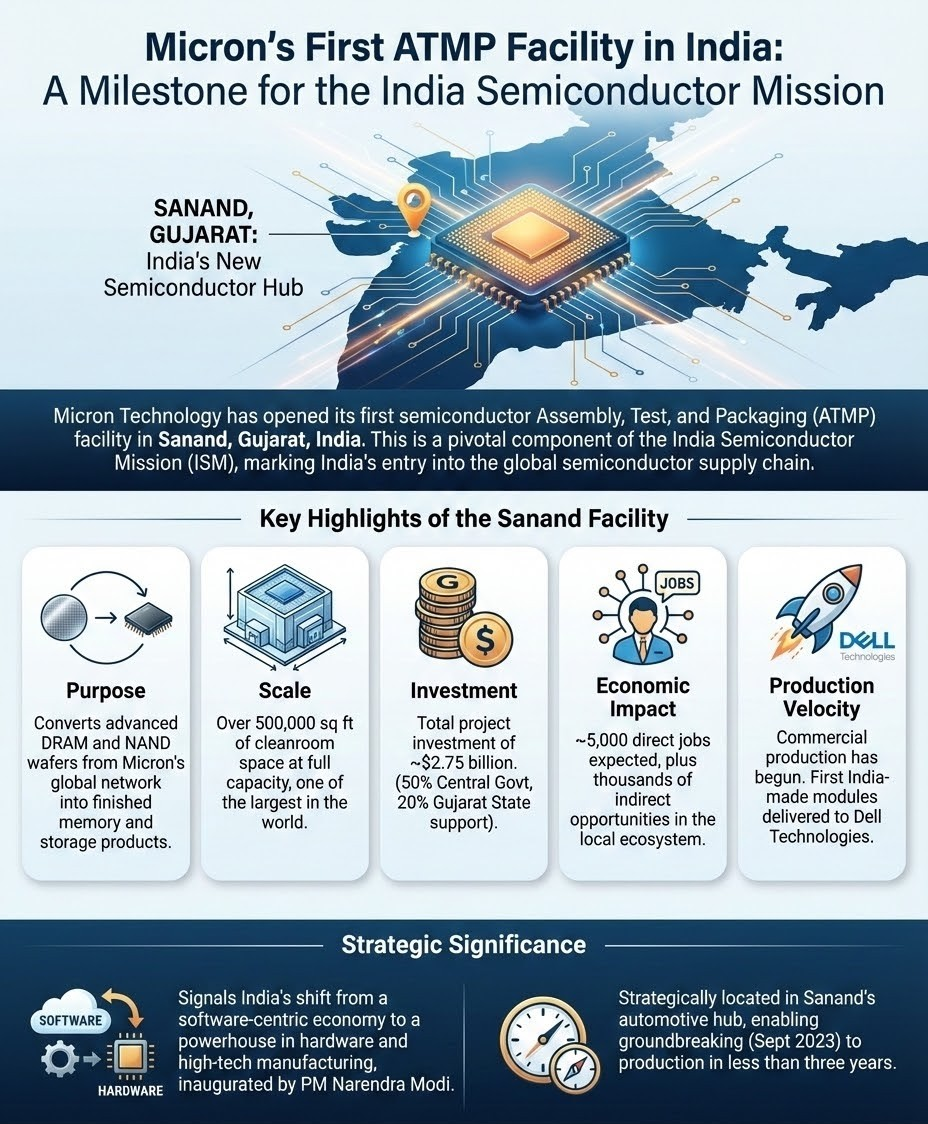
The Prime Minister recently inaugurated the Micron Technology's Semiconductor Assembly, Test, and Packaging (ATMP) facility in Gujarat.
|
Read all about: SEMICONDUCTOR SECTOR IN INDIA: CHALLENGES AND OPPORTUNITIES |
Micron Technology's Semiconductor Assembly, Test, and Packaging (ATMP) facility is India's first world-class commercial semiconductor assembly operation, located in Sanand, Gujarat.
Core Functions: It performs the critical final steps of semiconductor manufacturing: Assembly (thinning and dicing wafers into chips), Testing (verifying speed and capacity), and Packaging (mounting chips into finished modules).
End Products: The plant produces integrated circuit packages, memory modules, and Solid State Drives (SSDs) for global data centers, mobile devices, and AI applications.
 What is the Significance of Micron's Facility for India?
Strategic & Geopolitical Importance
Global Supply Chain Entry: The facility marks India’s official entry into the global semiconductor value chain, providing a "secure and reliable alternative" to traditional manufacturing hubs in East Asia.
India–US Collaboration: It is a project of the Pax Silica and TRUST initiatives, representing deep technological and diplomatic ties between the two democracies.
Reduced Import Dependence: By producing "Made-in-India" memory modules (DRAM and NAND), the plant helps reduce India's reliance on chip imports from China and Taiwan.
Economic & Industrial Impact
Catalyst for Ecosystem Growth: Much like Sanand’s rise as an automotive hub, this facility is expected to attract an entire ecosystem of suppliers, chemical providers, and logistics partners.
Job Creation: The project is projected to create 5,000 direct jobs and approximately 15,000 indirect employment opportunities.
Operationalizing the India Semiconductor Mission (ISM): As the first major project approved under ISM, its successful commercial launch validates India’s streamlined regulatory environment and "New India" policy-to-production speed.
Technological Leadership
AI Revolution Readiness: The facility focuses on high-performance memory crucial for Artificial Intelligence (AI) applications and data centres, aligning with the global surge in AI infrastructure demand.
World-Class Infrastructure: Featuring one of the world's largest raised-floor cleanrooms (around 500,000 sq. ft.), it demonstrates India's capability to host and operate high-tech manufacturing at a massive scale.
First Shipments: On its opening day, the facility delivered its first made-in-India memory modules to Dell Technologies for use in locally manufactured laptops.
Talent & Skill Development
Building a Talent Pipeline: Micron has partnered with Indian universities (e.g., PDEU, Namtech) to train thousands of engineers, supporting the government's goal of creating a workforce for advanced manufacturing.
R&D Integration: The plant leverages Micron's existing R&D presence in Hyderabad and Bengaluru, which has already contributed nearly 2,000 patents to the company's global portfolio.
India Semiconductor Mission (ISM) - Central Government
The primary driver is the Modified Semicon India Programme, which has a total financial outlay of ₹76,000 crore.
Gujarat Semiconductor Policy (2022-27) - State Government
Gujarat was the first Indian state to launch a dedicated Semiconductor Policy to provide additional "top-up" incentives:
Strategic International Frameworks
Complementary National Policies
Developing self-reliance in semiconductors is a strategic, economic, and technological imperative for India's future growth and security.
Economic Resilience
India's semiconductor market is projected to reach $100-110 billion by 2030, driven by domestic manufacturing efforts to reduce current import dependency (over 80%) and vulnerability to global supply chain shocks. (Source: PIB)
National Security
A domestic semiconductor manufacturing base is vital for modern defense, critical infrastructure, and government networks, ensuring sovereign control over these technologies.
Technological Sovereignty
As the global economy digitizes with technologies like AI, 5G, and IoT, control over the semiconductor value chain is essential for technological leadership and innovation.
What are the Major Challenges India Faces in this Sector?
High Capital & Infrastructure Needs
Semiconductor fabrication plants (fabs) require enormous capital and infrastructure, including uninterrupted high-quality power and vast amounts of ultrapure water (up to 10 million gallons per day for an average fab). (Source: WEF)
Talent & Skill Gap
While strong in chip design, India faces a shortage of skilled professionals in manufacturing and advanced packaging. The industry may face a shortfall of 250,000–300,000 professionals by 2027. (Source: CSIS)
Supply Chain Dependencies
The ecosystem relies heavily on imported raw materials, specialty gases, and precision equipment, with over 90% of these inputs being imported. (Source: CSIS)
Environmental Concerns
Chip manufacturing is resource-intensive and generates significant chemical waste and emissions. Sustainable practices are crucial for long-term growth.
Adopt a Phased Approach
Focusing on ATMP and OSAT (Outsourced Semiconductor Assembly and Test) to build foundational skills before moving to more complex wafer fabrication.
Strengthen the Entire Ecosystem
Shift focus from just fabs to the broader ecosystem, including equipment manufacturing, materials production, and deep-tech design startups.
Invest in Human Capital
Launch a national program in collaboration with industry and academia to create a skilled workforce for semiconductor manufacturing.
Prioritize Research & Development
Increase investment in R&D, which is currently low at 0.7% of GDP, to drive innovation in packaging, materials science, and manufacturing technologies.
Learn from Global Success Stories
Micron's ATMP facility marks a commendable start to India's semiconductor journey, which requires a strategic, phased approach focused on the entire ecosystem, human capital, and R&D to transition India into a global design and manufacturing hub.
Source: thenewsmill
|
PRACTICE QUESTION Q. With reference to the India Semiconductor Mission (ISM), consider the following statements: 1. It provides fiscal support of up to 75% of the project cost for setting up semiconductor fabs. 2. The mission aims to establish India as a global hub for electronics manufacturing and design. 3. The Micron Technology facility in Gujarat is the first major project to commence production under this mission. Which of the statements given above is/are correct? (a) 1 and 2 only (b) 2 and 3 only (c) 3 only (d) 1, 2 and 3 Answer: (b) Explanation: Statement 1 is incorrect: The ISM provides fiscal support of up to 50% of the project cost for setting up semiconductor and display fabrication units (fabs) on a pari-passu basis. Statement 2 is correct: The India Semiconductor Mission (ISM) was launched to build a sustainable semiconductor and display ecosystem in the country, with the primary objective of positioning India as a global hub for electronics manufacturing and design. Statement 3 is correct: The Micron Technology assembly, testing, marking, and packaging (ATMP) facility in Sanand, Gujarat, is the first major project under the mission to commence progress and production-related activities. |
Launched in 2021 with an outlay of ₹76,000 crore, the ISM is the Government of India's flagship initiative to build a comprehensive semiconductor and display ecosystem. It provides significant fiscal support (up to 50% of project cost) to attract investments in semiconductor fabrication, assembly, and design.
ATMP stands for Assembly, Test, and Packaging. It is the final and crucial stage of the semiconductor manufacturing process where silicon wafers are cut, assembled into protective packages, and tested to ensure they function correctly before being used in electronic devices.
The primary challenges include ensuring reliable infrastructure like uninterrupted power and ultra-pure water, bridging the skilled workforce gap for high-end manufacturing, reducing dependency on imported raw materials like specialty chemicals and gases, and increasing investment in the domestic R&D ecosystem.
© 2026 iasgyan. All right reserved