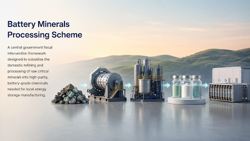
Description
Source: Hindu
Disclaimer: Copyright infringement not intended.
Context
- Semiconductor chip manufacturing capabilities are currently limited to very few regions in the world.
- The TATA group has partnered with Taiwan’s Powerchip Semiconductor Manufacturing Corporation (PSMC) to set-up a 300mm wafer fabrication plant in Gujarat.
- It will roll out its first 28nm chip in 2026.
- Two assembly and test plants in Gujarat and Assam have also been recently approved by the Government of India.
Details
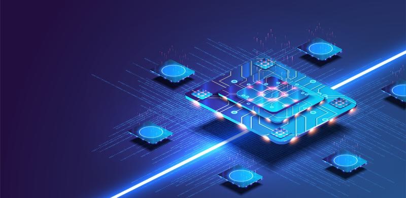
- A semiconductor chip, also known as an integrated circuit (IC) or microchip, is a small electronic device made from a semiconductor material, typically silicon.
- It contains electronic components such as transistors, resistors, and capacitors, all fabricated on a single piece of semiconductor material
What is a Transistor?
- A transistor is a semiconductor device that can amplify or switch electronic signals.
- It consists of three layers of semiconductor material: the emitter, base, and collector.
- In its basic form, a transistor acts as a switch, controlling the flow of current between its emitter and collector terminals based on the voltage applied to its base terminal.
- Transistors are fundamental components of integrated circuits, enabling the creation of complex electronic circuits on semiconductor chips.
- They can also serve as amplifiers, boosting the strength of weak electronic signals, and are essential for various applications, including wireless communication technologies and digital logic circuits.
Semiconductor Material Preparation
- Silicon Wafer Production:
- Silicon ingots are grown using methods like the Czochralski or Float-Zone process, ensuring high purity.
- The ingots are then sliced into thin, circular discs known as silicon wafers, typically several inches in diameter.
- Slicing:
- Precision sawing or slicing techniques are employed to cut the silicon ingots into wafers of uniform thickness.
- The surfaces of the wafers are polished to achieve smoothness, critical for subsequent processing steps.

Semiconductor Fabrication (Fabrication Technology)
- Photolithography:
- Photolithography involves using masks containing circuit patterns and exposing them to UV light through a photoresist-coated wafer.
- The exposed areas of the photoresist become soluble and are removed, leaving behind the desired circuit pattern on the wafer.
- Doping:
- Dopants, such as phosphorus or boron, are introduced into specific regions of the silicon wafer to modify its electrical properties.
- Techniques like ion implantation or diffusion are used to precisely control the dopant concentration and distribution.
- Layer Deposition:
- Insulating (e.g., silicon dioxide) and conducting (e.g., polysilicon, metal) materials are deposited onto the wafer's surface using methods like chemical vapor deposition (CVD) or physical vapor deposition (PVD).
- These layers form the building blocks for creating transistors, interconnects, and other electronic components.
Wafer Dicing and Chip Packaging
- Dicing:
- After the fabrication process, the wafer is diced into individual chips using diamond saws or laser cutting techniques.
- Each chip contains multiple copies of the integrated circuit pattern created during fabrication.
- Packaging:
- Individual chips are mounted onto lead frames or substrates and encapsulated in protective materials such as epoxy resin or ceramic.
- Bond wires or flip-chip connections are used to establish electrical connections between the chip and the package leads.
- Testing:
- Packaged chips undergo rigorous testing to ensure functionality and reliability.
- Functional testing verifies that the chip performs its intended operations, while stress testing assesses its performance under extreme conditions such as temperature and voltage variations.
Role of the Transistor in Semiconductor Revolution
- Replacement of Vacuum Tubes: Transistors replaced bulky and power-hungry vacuum tubes in electronic devices, leading to smaller, more efficient circuits.
- Fundamental Building Blocks: Transistors serve as the basic building blocks of integrated circuits, enabling the creation of complex digital and analog functions.
- Versatility: Transistors can function as switches, amplifiers, or voltage regulators, making them essential components in virtually all electronic devices.
Semiconductor Miniaturization
- Feature Size Trend:
- The semiconductor industry has continuously reduced the size of transistors and other components to increase performance and reduce costs.
- Terms like "45nm," "28nm," or "16nm" refer to the minimum feature size achievable using a particular fabrication technology.
- Advantages:
- Smaller feature sizes allow for higher transistor density, faster switching speeds, and lower power consumption, driving advancements in computing and telecommunications.

Conclusion
- Semiconductor manufacturing requires expertise in diverse fields, including materials science, chemical engineering, and automation, presenting opportunities for professionals from various disciplines to contribute to the industry's growth and innovation.
Must Read Articles:
Semiconductor Manufacturing in India
Semiconductors
Sources:
News 18
|
PRACTICE QUESTION
Q. Transistors serve as the basic building blocks of integrated circuits. Comment. (150 Words)
|