Crystals are normally rigid, stiff structures. But, recently researchers from University of Hyderabad have shown how crystals can be sliced and even bent using atomic force microscopy. Manipulating them with precision and control comes in very useful in the field of nanophotonics.
| A crystal or crystalline solid is a solid material whose constituents (such as atoms, molecules, or ions) are arranged in a highly ordered microscopic structure, forming a crystal lattice that extends in all directions. |
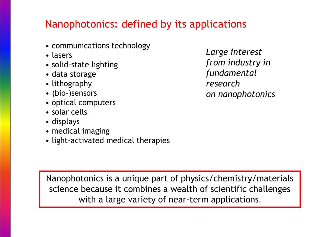
Nanophotonics studies how light behaves at the nano-scale and how it interacts with nanosized objects. It is a branch of optics, optical engineering, electrical engineering, and nanotechnology.
Think of nanophotonics as the study of understanding and engineering light at a very, very small scale, or also known as a nanometer scale. The word photonics in nanophotonics basically refer to photons, the building block of light.
By understanding how these photons behave on a nanoscale, we can start controlling and manipulating their interactions with matter giving rise to ingenious inventions, such as a better way for cancer imaging or a potential solution for room-temperature quantum computers!
Thus, Nanophotonics is a qualitative, emerging field where the aim is to go beyond electronics and build up circuits driven entirely by photons (light).
If the technique can be successfully developed, this can achieve an unprecedented level of miniaturisation. It will pave the way to all-optical technology such as pliable, wearable devices operated by light entirely.
Quantum optics
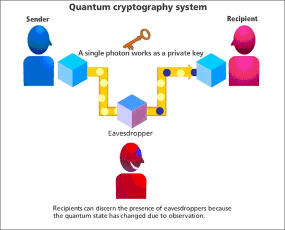
The opportunity in nanoscale quantum optics lies in developing components for quantum communication and quantum computing. Quantum cryptography is the science of using quantum mechanical properties to perform cryptographic tasks and provides an intrinsically secure and unbreakable code.
Also, Quantum computers promise an exponential speed-up of important processes, allowing them to have massive parallel computation to solve important problems.
Nanophotonics can help actualize these technologies by making them readily available for room temperature operation! In fact, scientists at MIT recently developed a new photonic device, using a silicon crystal to enable photon-photon interactions at room temperature.

Photonic device
In quantum computers, there is a strange physical property called superposition. In this, a quantum particle can occupy two contradictory states at the same time. For instance, the spin, or magnetic orientation in space, of an electron can be up and down at the same time. Similarly, the polarization of a single photon can be horizontal and vertical at the same time. If a string of qubits (the quantum analog of bits for classical computers) is in superposition, it can canvass solutions to a problem simultaneously, leading to the promise of incredible speedups.
As protons aren’t susceptible to interactions with the environment, they are great at maintaining superposition, but for the same reason, they are difficult to control. This is where the photonic device comes in: If a single photon enters their device, it will pass through unimpeded. But if two photons — in the right quantum states — try to enter the device, they’ll be reflected back. Thus the quantum state of one proton can be thought of as controlling the quantum state of the others.
Photonic nanomaterials
Another exciting example for photonic nanomaterials is quantum dots (QDs). As the name implies, think of quantum dots as incredibly small matter that is concentrated in a single dot. In other words, if you set the constraints for a nanomaterial, put it inside an imaginary box and confine it in all three dimensions, you will get a sphere that ranges a few nanometers.
Thus, quantum dot is an epitome of such sphere in the field of nanotechnology and is zero-dimensional. They are composed of semiconducting materials such as silicon or Cd, meaning that they are neither strictly an insulator or conductor but chemically behave like both. Due to their atom-like behaviors, QDs are often used for special optical properties that can be employed for fabricating optical probes for biological and medical imaging.
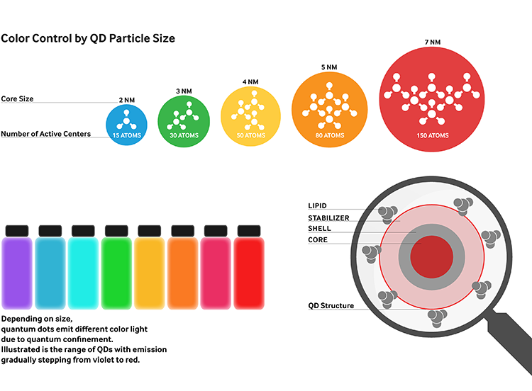
One promising application of QDs is they can revolutionize the way we diagnose and treat cancer today. QD molecular imaging introduces new way of seeing biologic processes at work within cells and in small animals in real time, which is in itself an incredible feat.
Quantum dots emitting different wavelengths are visible after injection into a mouse.
A representation of quantum dot based single cell imaging cytometry can help determine breast cancer subtypes.
A similar technique can be used for cancer patients, who can be injected with a cocktail of QDs that would “label” cancerous cells. Once they’re gathered at the tumor site, the positrons emitted from the QDs could be imaged with PET scanner which would indicate the presence and location of a tumor. An “optical barcode” of the different colored qdots could help doctors identify tumor type and stage by allowing them to see differing levels of various tumor markers. QDs imaging can potentially replace the lengthy and costly process of how we are currently treating cancer today!
The Superpowers of Light: Virtual Photons
In classical mechanics, light is described as coupled electric and magnetic fields propagating through space as a traveling wave.
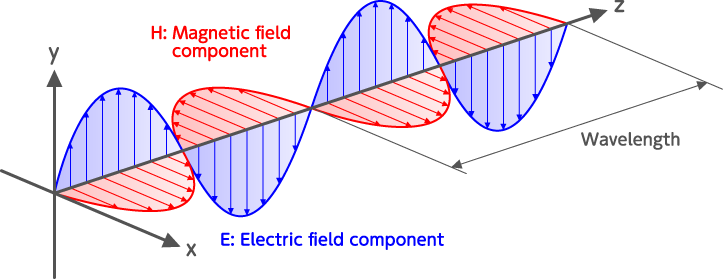
However, this wave theory is not sufficient to explain the properties of light at very low intensities or at a nanoscale. Thus, people have turned to quantum theory describes light as consisting of discrete packets of energy, known as photons.
As light behaves as both waves and particles physicists have merged these two classical theories together and introduced a more comprehensive one, often known as quantum electrodynamics (QED).
Let’s break it down and step-by-step understand what QED talks about!
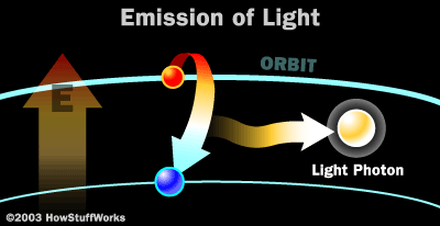
In classical mechanics, we become aware of field forces, such as gravitation force or electromagnetic force. The key thing we need to understand is that these fields impart forces on the object, causing it to accelerate. For example, the Earth has a gravitational field, which causes the apple to experience a gravitational force downwards and fall from the tree.
Quantum theory redefines these field forces by describing forces as the interactions between particles. Instead of force being mediated by light, Richard Feynman hypothesized that it is mediated by something called virtual photons.

In the Chalmers scientists’ experiments, virtual photons bounce off a “mirror” that vibrates at a speed that is almost as high as the speed of light.
Now, these virtual particles are actually quite interesting: They are able to come in and out of existence for brief instants. Due to this property, they are considered as virtual, since they don’t exist with the same permanence as ordinary particles that makeup matters. Once these virtual particles interact with charged particles, like photons or electrons, they cause these particles to bounce off and change direction, as if they were affected by a force. In short, force is replaced by interactions between virtual and real particles.
Although it sounds absolutely absurd that a particle can pop out of nowhere, virtual particles can explain many phenomena in nanoscale photonics.
Casimir-Polder effect
Casimir-Podler effect, basically refers to the attraction between two objects should they come within 100 nm of each other. The two objects were placed in a vacuum, which contains empty space.
Surprisingly, however, the empty space isn’t really empty. It roils and boils with something known as quantum fluctuations, occasionally spitting out pairs of “virtual” elementary particles. Think of it as waves of particles appearing and vanishing all the time. These virtual particles annihilate and disappear back into the quantum vacuum so quickly that the apparent violation of energy conservation incurred by their creation can’t be observed directly.
Strong Casimir force reduction through metallic surface nanostructuring
Although practical applications of the Casimir effects have not been found, it is important for researchers and manufacturers to keep in mind to design effective nanoscale devices that we use in, say computer chips, today!
Optical binding
Another important way of controlling light is through optical binding. When two walls of nanoparticles interact with a plane wave, the optical binding force occurs. As a result, the locations of the two nanoparticles become fixed.
What happens consequently is a potential well occur, trapping more nanoparticles and making the structure more stable. Compared to microscale particles, stronger trapping forces are required to overcome the thermal forces for fine control of objects at the nanoscale. Thus, optical binding has potential applications in trapping small particles and assembling nanostructures.
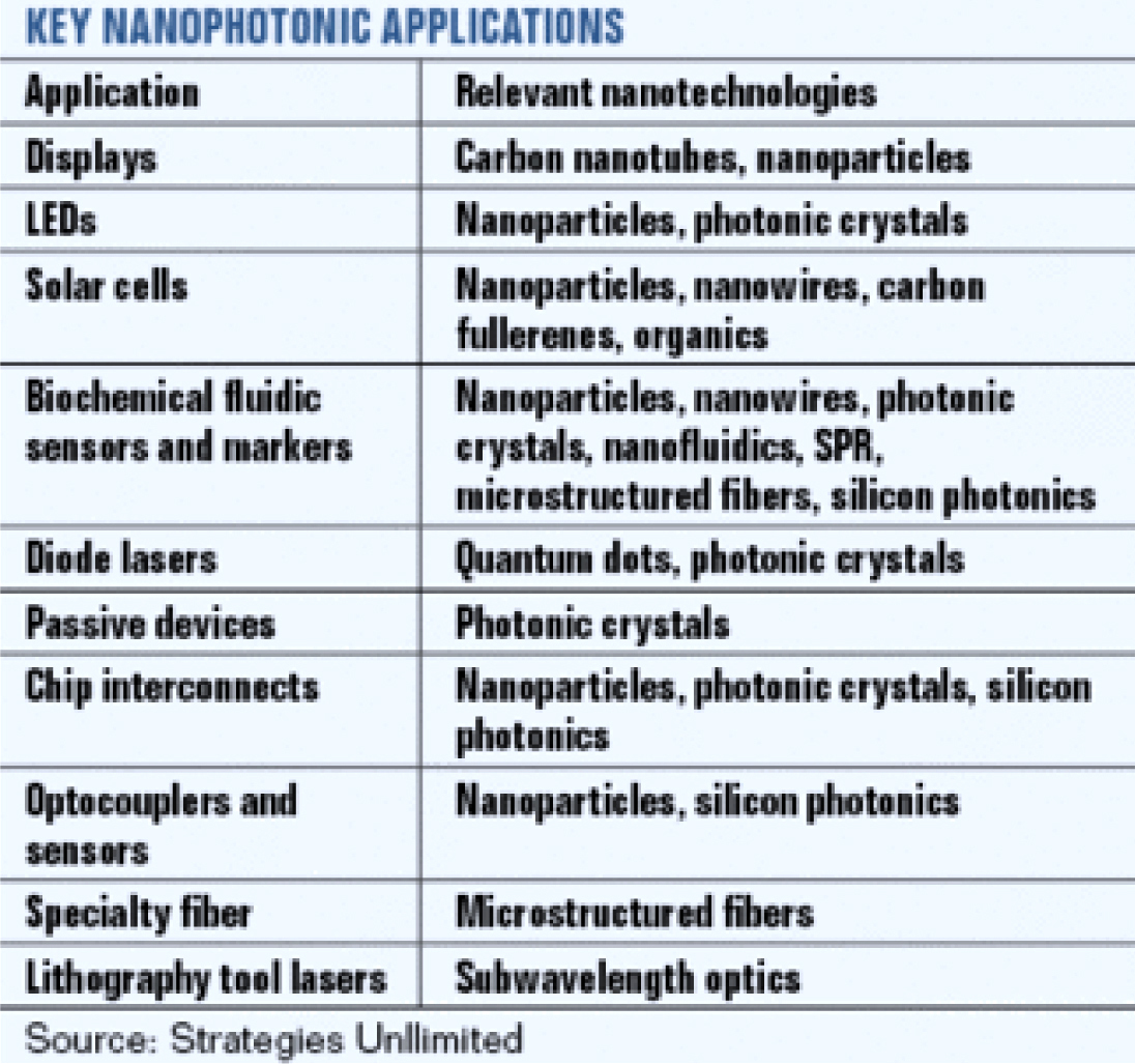
It is possible to design nanometer scale devices to slow down, enhance, produce, or manipulate light by understanding how light behaves as it travels through materials at the nanometer scale. Two applications where nanophotonics have had an impact on society are devices used in optical switching for telecommunications and Organic Light Emitting Diodes (OLEDs) used in display technology and lighting.
Microresonators
Recently, the Hyderabad group Researchers have extended the atomic force microscopy technique to deliberately move, bend, slice or cleave and transfer (from one substrate to another) micro-sized waveguiding crystals. They have also shown how other crucial elements needed for nanophotonics can be developed using this technique. “Not only crystals but also polymer microcavities or microresonators (light-trapping elements) can be precisely manipulated to create photonic structures.
The researchers have named this technique “mechanophotonics” as this method can be used to generate the basic elements needed to build up a photonic integrated circuit.
Usually photonic integrated circuits are made using silicon, silicon-based and metallic materials using electron beam lithography. This group on the other hand uses organic materials and atomic force microscopy to manipulate them.
The field of Nanophotonics is in its infancy. Next, the researchers are planning to fabricate high-density photonic circuits using organic passive, active and energy transfer mechanisms.
By squeezing light down to the nanoscale to exploit optical phenomena, nanophotonics can challenge existing technological limits and help deliver superior photonic devices.

© 2026 iasgyan. All right reserved